Capacitance sensors based on fixed and variable-area silicon membranes are useful for multi-range pressure and acoustic sensing applications.
Our inductively-coupled plasma deep reactive
ion etcher is being used to fabricate
biomedical devices for testing and research.
Custom microfabrication of medical implants,
lab-on-a-chip platforms, biohazard test devices,
and medical test and
drug delivery systems.
Silicon v-grooves and micro-optical benches are used for precise alignment of fiber-optic telecommunications and laser-based systems for many applications.
Application-specific membranes and arrays are built
on silicon membrane platforms for microfiltration, calibration grids, and sensing arrays.
We work with customers through purchase orders
and R&D/engineering contracts. We handle micro-fabrication jobs of varying sizes and scopes, from R&D, to small-lot prototypes, to volume manufacturing.
nanostructures
Custom Microfabrication
|
|
Capabilities
|
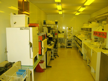
Fabrication Facility
- Total facility size 4,200 square feet
- Clean rooms 1,000 square feet
- Capacity
- R&D and prototype lots
- OEM production
- 200-400 wafers per month
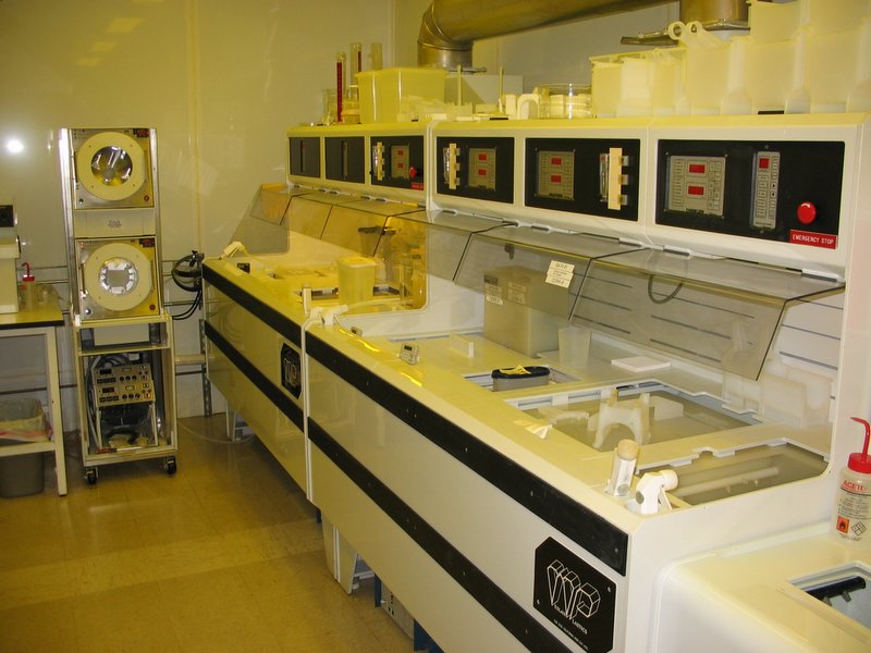
Clean Room Fabrication Processes
- Photolithography
- Substrate sizes up to 6"
- Photomask and shadowmask layout
- Positive and negative resists
- Lift-off
- Front-to-back alignment
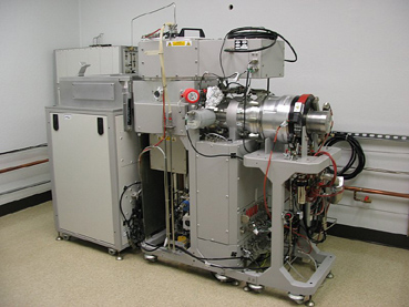
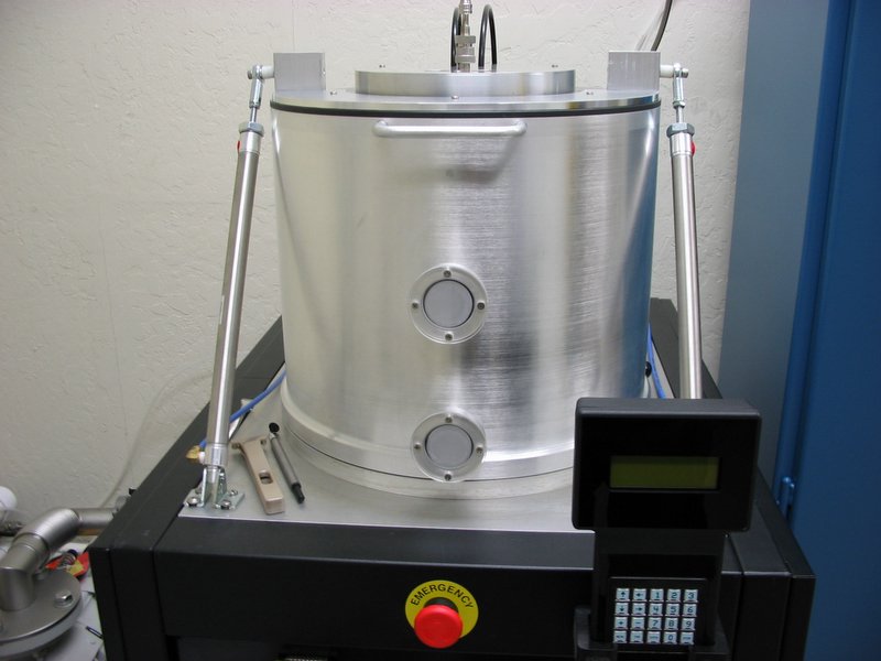
- DRIE for deep silicon etch
- STS inductively coupled plasma (DRIE)
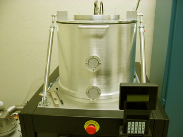
- Thin Film coatings
- LPCVD and PECVD dielectrics
- TiNi thin film shape memory
- Sputtered and evaporated metals
- Thermal oxide
- Other processes
- Reactive ion etch
- Barrel etch
- Wet chemical clean
- Hard masks and etch stops
- Wafer bonding -- anodic, silicon, glass
- Dicing and trenching
- Special processes
- Membrane fabrication
- Bulk micromachining of silicon and glass by
wet etch
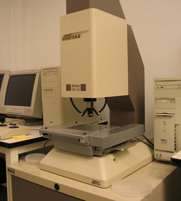
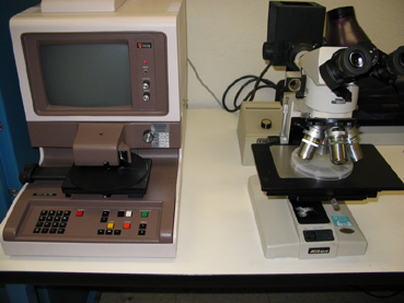
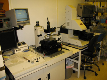
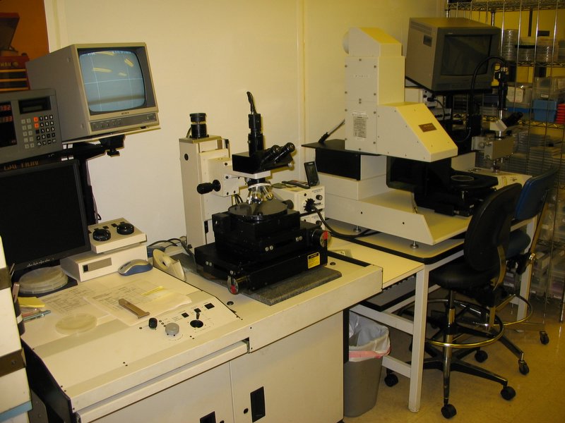
- Measurements and QA
|
|
| |
|
Copyright
© 2016 Nanostructures, Inc. 3070 Lawrence
Expy. Santa Clara, CA 95051
info@nanostructures.com, Phone:(408)733-4345
We accept American Express
 |
